

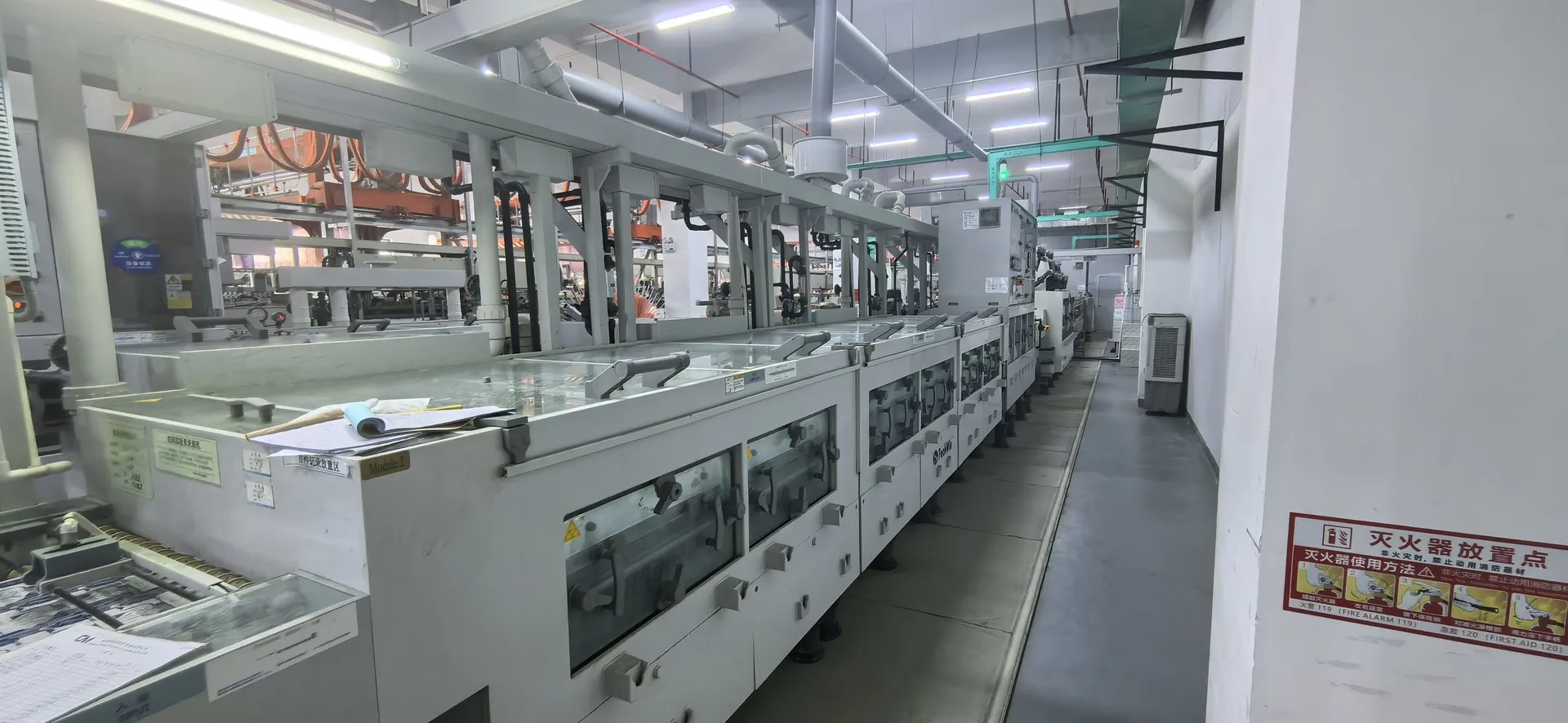
PCB Manufacturing Capabilities
Capability limits for rigid, rigid-flex, flexible and high-frequency boards. Specific values for your design are confirmed against your files and the assigned production scope.
Capability tables
Select a board type. Prototype and mass-production values are never interchangeable — plan production on the mass-production column.
| Parameter | Prototype | Mass production |
|---|---|---|
| Layer count (max) | 48L | 36L |
| Finished board thickness | 0.2–15.0 mm | 0.3–7.0 mm |
| Thickness tolerance | ±8% | ±8% |
| Min trace / space | 1.5 / 1.5 mil | 2 / 2 mil |
| Min hole-to-trace clearance | 5 mil | 5 mil |
| Copper weight | 1–12 oz | 1/3–8 oz |
| Layer registration accuracy | 0.8 mil | 1 mil |
| Min through-hole diameter | 0.075 mm | 0.10 mm |
| Min blind / buried via diameter | 0.05 mm | 0.075 mm |
| Max aspect ratio | 35:1 | 30:1 |
| Etching tolerance | ±10% / ±0.8 mil | ±10% / ±1 mil |
| Min solder mask bridge | 2 mil | 3 mil |
| Impedance control tolerance | ±5% | ±7% |
| HDI level | 9th order | 5th order |
| Surface finish | ENIG, hard gold, immersion tin, immersion silver, OSP, carbon | ENIG, hard gold, immersion tin, immersion silver, OSP, carbon |
| Material types | Shengyi, Taiwan Union, ITEQ, Nan Ya, Rogers, Panasonic, Isola (Tg135 / Tg150 / Tg170, CAF / CTI>600, halogen-free) | Same material families as prototype |
Source: ShinePCB capability workbook, 2025 values. Prototype and mass-production values are listed separately and are not interchangeable. Every value is confirmed against your files, the selected material and the assigned facility during engineering review.
| Parameter | Prototype | Mass production |
|---|---|---|
| Layer count (max) | 20L | 18L |
| Panel size | 400 × 540 mm | 400 × 540 mm |
| Finished board thickness | 0.25–5.0 mm | 0.25–3.2 mm |
| Min trace / space | 1.5 / 1.5 mil | 2 / 2 mil |
| Min hole-to-trace clearance | 4 mil | 5 mil |
| Copper weight | 1/3–3 oz | 1/3–2 oz |
| Layer registration accuracy | 0.8 mil | 1 mil |
| Min through-hole diameter | 0.075 mm | 0.10 mm |
| Min laser via diameter | 0.05 mm | 0.05 mm |
| Max aspect ratio | 16:1 | 12:1 |
| Etching tolerance | ±10% / ±0.8 mil | ±10% / ±1 mil |
| Min solder mask bridge | 2 mil | 3 mil |
| Impedance control tolerance | ±5% | ±7% |
| Surface finish | ENIG, hard gold, immersion tin, immersion silver, OSP, carbon | ENIG, hard gold, immersion tin, immersion silver, OSP |
| Supported structures | Single-sided core, symmetrical and asymmetrical stack-ups, multilayer, gold finger, air gap, HDI, build-up, bookbinder, high-speed design | Same structures as prototype |
| Material types | Shengyi, Ventec, Taiwan Union, ITEQ, Panasonic, Rogers, Isola, Arlon | Same material families as prototype |
Source: ShinePCB capability workbook, 2025 values. Prototype and mass-production values are listed separately and are not interchangeable. Every value is confirmed against your files, the selected material and the assigned facility during engineering review.
| Parameter | Prototype | Mass production |
|---|---|---|
| Layer count (max) | 12 | 16 |
| Min dielectric thickness | 12.5 µm | 12.5 µm |
| Min BGA pitch | 150 µm | 100 µm |
| Min board thickness | 50 µm | 50 µm |
| Max panel size | 610 × 1200 mm | 610 × 1200 mm |
| Base copper thickness | 9–35 µm | 6–35 µm |
| Min trace / space | 40 / 40 µm | 35 / 35 µm |
| Pattern registration tolerance | ±50 µm | ±20 µm |
| Min pattern-to-edge clearance | 0.10 mm | 0.07 mm |
| Etching tolerance | ±20 µm | ±15 µm |
| Min through-hole diameter | 0.10 mm | 0.075 mm |
| Min blind via diameter | 0.05 mm | 0.05 mm |
| Hole diameter tolerance | ±0.05 mm | ±0.05 mm |
| Impedance control tolerance | ±10% | ±5% |
| Outline tolerance | ±0.10 mm | ±0.05 mm |
| Surface finish | HASL, ENIG, immersion silver, OSP, ENEPIG, hard gold | HASL, ENIG, immersion silver, OSP, ENEPIG, hard gold |
| Stiffener type | FR-4, PI, stainless steel | FR-4, PI, stainless steel |
| Stiffener registration tolerance | ±0.20 mm | ±0.10 mm |
| HDI capability | 4-layer any-layer interconnect | 6-layer any-layer interconnect |
| LCP material | Supported | Supported |
Source: ShinePCB capability workbook (FPC sheet has no year column). Prototype and mass-production values are listed separately and are not interchangeable. Every value is confirmed against your files, the selected material and the assigned facility during engineering review.
| Parameter | Prototype | Mass production |
|---|---|---|
| Material system | PTFE, hydrocarbon resin, other materials | PTFE + ceramic, PTFE + glass fiber + ceramic, PTFE + glass fiber |
| Layer count (max) | 24L | 20L |
| Panel size (max) | 850 × 700 mm | 720 × 650 mm |
| Profile tolerance | ±0.05 mm | ±0.10 mm |
| Slot tolerance | Normal slot ±0.08 mm, routed slot ±0.10 mm | Normal slot ±0.10 mm, routed slot ±0.13 mm |
| Layer registration | 2 mil | 3 mil |
| Hybrid lamination | PTFE + glass ceramic + FR-4 | PTFE + glass ceramic + FR-4 |
| Min hole size | 0.075 mm | 0.10 mm |
| Min hole spacing | 0.20 mm | 0.25 mm |
| Hole diameter tolerance | ±0.05 mm | ±0.075 mm |
| Max aspect ratio | 16:1 | 12:1 |
| Hole copper uniformity | COV ≤ 5% | COV ≤ 7% |
| Resin-filled via aspect ratio | 12:1 | 12:1 |
| Resin-filled via type | Through hole / blind via | Through hole / blind via |
| Trace width tolerance | ±0.6 mil | ±1 mil |
| Impedance tolerance | ±5% | ±8% |
| Warpage | 0.50% | 0.75% |
| Special processes | POFV (VIPPO), sequential lamination, local lamination, long/short gold finger, counterbore, back drill, side metallization, N+N structure, edge plating, thick copper, HDI | Same processes as prototype |
| Approved material brands | Shengyi, ITEQ, Taiwan Union, Panasonic (M4/M6/M7/M8), Rogers, Taconic, Wangling, Ventec, Isola | Same brands as prototype |
Source: ShinePCB capability workbook (high-frequency & high-speed sheet has no year column). Prototype and mass-production values are listed separately and are not interchangeable. Every value is confirmed against your files, the selected material and the assigned facility during engineering review.
Factory-wide parameters
| Item | Value |
|---|---|
| Max board size | 1 × 1 m |
| Minimum board thickness | 0.20 mm |
| Minimum drill diameter | Φ0.15 mm |
| Drill hole tolerance | ±0.05 mm |
| Warpage control | 0.75% |
| Impedance tolerance (general) | ±10% |
| Quality inspection | AOI, X-ray, flying probe test, impedance testing, final electrical test |
| Pre-shipment inspection | 100% |
| In-house PCB laboratory | Supported, 20+ sets of lab equipment |
Source: ShinePCB capability workbook, factory-general rows (same value for prototype and mass production).
Product line and advanced processes
Supported board types
- Single and double-sided PCB
- Multilayer PCB (4–48L)
- HDI PCB
- High-frequency and RF microwave PCB
- High-speed PCB
- Flexible PCB (FPC)
- Rigid-flex PCB
- Heavy copper PCB
- Metal core PCB (aluminum / copper base)
- Ceramic PCB
- Backplane PCB
- Prototype and quick-turn
Advanced processes
- Solder mask plugged via
- Resin plugged via
- Plated via fill
- Copper filled via
- POFV / VIPPO
- Sequential lamination
- Local hybrid lamination
- N+N structure
- Long / short gold finger
- Counterbore
- Back drilling
- Sidewall metallization
- Edge plating
- Carbon ink
- High layer count (up to 48L)
Values not yet published
Some parameters — for example back-drill stub length, routed outline tolerance, maximum backplane size and metal core thermal conductivity — have no approved value in the capability workbook yet. They are confirmed per project during engineering review.
From prototype to production
Every order follows the same controlled sequence. Prototype and production requirements are reviewed separately.
File review
Gerber or ODB++, drill data, drawing and quantities are checked for completeness.
Engineering questions
Open points on manufacturability, materials or special processes are sent before quotation.
Stack-up and material
Construction, laminate and finish are confirmed with you and written into the order.
Fabrication
The order is released to the facility whose process and qualification fit the requirements.
Inspection and test
Inspection and electrical test follow the methods agreed for your order.
Packing and delivery
Boards are packed and shipped under the confirmed delivery terms.
What to send for a PCB review
Start with the details you have — engineering will request anything else needed for the review.
Files and details for a PCB review
- Gerber (RS-274X) or ODB++ data with drill files
- Fabrication drawing with material, thickness and finish
- Stack-up and impedance targets, if any
- Quantity for prototype and for production
- Special requirements such as IPC class, testing or packaging
Technical files stay private
Customer Gerber, BOM and design data are managed under an ISO/IEC 27001 information security system and shared only within your project.